What is Diode? Diode Symbol Circuit, Types & Characteristics
What is Diode : A diode is
defined as a two-terminal electronic component, which conducts current in only
one direction (so long as it operates within a specified voltage).
What is Diode : A diode is defined as a two-terminal electronic component, which conducts current in only one direction (so long as it operates within a specified voltage).
What is Diode
The symbol
of a diode is shown below. Arrowheads point in the direction of conventional
current flow in a forward-biased position. This means that the anode is
connected to the P side and the cathode is connected to the N side
We can make
a simple PN junction diode by doping pentavalent or donor impurities in one
part and trident or acceptor impurities in another part of silicon or germanium
crystal blocks.
P-type and
N-type junction is the simplest form of semiconductor diode. Under ideal
circumstances, this P.N. junction
behaves as a short circuit when it is biased, and as an open circuit when it is
in reverse bias. The name diode is derived from "di-ode" which means
a device consisting of two electrodes. Diodes are used in all electronics
projects and are included in all of the best Arduino starter kits.
diodes to conduct electricity when a certain
threshold voltage is present in the forward direction (i.e. the "low
resistance" direction). The diode is called "forward biased"
when the current flows in this direction. When connected to a circuit in the
reverse direction (ie "high resistance" direction), the diode is
called "reverse biased".
These form a
PN junction in the central part of the doping block. We can also form PN
junctions by connecting with p-type semiconductors and n-type semiconductors
with a special fabrication technique. Connected to the P-type is the terminal
anode. and N-type is the terminal
cathode
How to work diode
The working
principle of a diode depends on the interaction of n-type and p-type
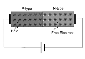
semiconductors. An n-type semiconductor has a lot of free electrons and a very
small number of holes. In other words, we can say that the concentration of
free electrons is high and the number of holes is very low in n-type semiconductors.
The free
electrons in the n-type semiconductor are known as the majority charge
carriers and the holes in the n-type semiconductor are referred to as minority
charge carriers.
A P-type semiconductor has a high concentration of pores and a low concentration of free
electrons. The holes in the p-type semiconductor are the majority charge
carriers, and the free electrons in the p-type semiconductor are the minority
charge carriers.
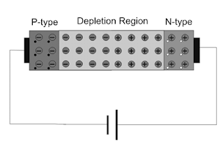
Now let us see what happens when an n-type region and a p-type region come into contact. Here, due to the concentration difference, the majority of carriers disperse from one side to the other. Since the concentration of pores in the P-type region is high and it is low in The N-type region, the holes
N-type the region, the holes begin to propagate from the P-type region to the N-type
region.
Again the concentration of free electrons is higher in the n-type region and it is lower
in the p-type region for this reason, free electrons start to propagate
from the n-type region to the p-type region.
Spreading
the free electrons from the n-type region to the p-type region will recombine
with the holes available there and create open negative ions in the p-type
region. In the same way, holes extending from the p-type region to the n-type region will recombine with the free electrons available there and form open
positive ions in the n-type region.
Forward biased diode
Now let us
see what happens if the positive terminal of a source is connected to the
p-type side and the negative terminal of the source is connected to the n-type
side of the diode and if we slowly increase the voltage of this source to zero.
A the
beginning, there is no current through the diode. This is because although an
external electric field is applied across the diode, the majority of charge
carriers do not get enough of the external field effect. As we reported the
depletion region acts as a potential barrier against the majority of carriers.
This potential barrier is called the forward potential barrier. The majority of
charge carriers begin crossing the forward potential barrier only when the
value of the voltage externally exerted outside the junction exceeds the capacity of the forward resistor. For silicon diodes, the forward barrier
capacity is 0.7 volts and for germanium diodes, it is 0.3 volts.
Reverse biased diode
Now let us
see what happens if we connect the negative terminal of the voltage source to
the diode of the p-type side and the positive terminal of the voltage source to
the n-type side. In that case, due to the electrostatic attraction of the negative potential of the source, the hole in the p-type region will be shifted
more from the junction leaving more open negative ions from the junction.
In the same
way, free electrons in the n-type region will be shifted away from the
junction and more open positive ions will be left in the junction toward the positive terminal of the voltage source.


0 Comments
Leave a Reply...